How does P10 Led Panel Work? | Working Principle and calculations
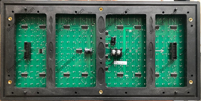
P10 Led Panel 32x16 consist of 512 leds. There are 2 connectors, called Hub1.2 (8x12 male header) and 5v power connector. Hub1.2 placed left side of the board shown in image below is input, right one is the connector to connect another p10 panels input.
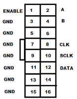
Pin definition of Hub1.2 is shown in image. ENABLE pin is the pin which allows you to control the panel is working state or stop state. Panel enables when it is driven a HIGH signal, When it is driven low it does not matter another pin states, panel stops working.
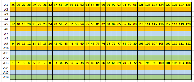
A, B are row selectors, this pins represent a 2 bit binary number allow you to select one of four rows in a sequence. Selecting a row means that, the leds on the selected row are powering their anod pins. There are 16 rows in total(A1-A16), and they are in a group of 4. Each group of rows are represented with the same color in the images below. Look at the table, driving A and B with a LOW signal means selecting rows labelled A1,A5,A9 and A13.
Data pin is generally used like SPI protocol's, data pin. In fact this pin is serial data input of the selected row. Every row in a panel has 128 leds and this means we have 128 bit serial data to drive a row. The zero bits of this data set, connect the cathode pins of leds with same index number to gnd. This means, driven low bits lights up the leds.
CLK pin shifts the current level of data input every pulse signal, sending whole data of a row need 128 pulse to complete. The numbers in the image 1 to 128 represents data bits of a row, You can see that the first bit of data numbered 1, the last data sended is numbered 128. Sending data is not activate GND connections of cathode pins of leds, this just sending process.
When you complete sending 128 bits data of a row, then you should send a pulse signal to activate the the data to row on SCLK pin.
The Summary of Process
- Drive LOW Enable pin.
- Select a row on AB pins
- Make your data bit ready on data pin
- Send a pulse to CLK pin to shift your data bit into shift register
- Repeat step 3, for 128 bit
- Send a pulse on SCLK pin to active data on shift register
- go to second step and select next row
- repeat whole process minimum 25 times for a second ( this is FPS value of your scanning topology)
Frequency Calculations
CLK frequency -> 128 bit data for a row, 4 total rows, 25 frame per second 12,8KHz.
SCLK frequency -> 4 rows and 25 FPS 100 Hz.
How to set brighness?
Brightness can be set by sending PWM signal on the Enable pin.


Comments
Post a Comment
You can share your experience, or ask anything about the topic, Let's write ;)